





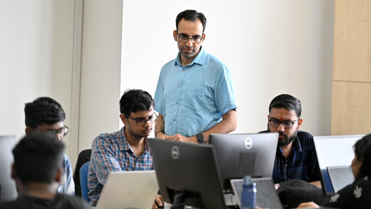
In 2002, Yuan Taur, a professor at the University of California, San Diego, who by then was already a doyen in electrical engineering circles, asked a master’s degree student from India, Anuj Grover, to stay on and do a PhD under his supervision. It was a major opportunity — Grover would be working on device design. But he hesitated, knowing that there were few job prospects to pursue based on this work were he to come back to India — and he wanted to come back. He turned the offer down.
“Today, if I had to make that same decision, I would have jumped at the opportunity,” Grover says from his office at the Indraprastha Institute of Information Technology (IIIT) Delhi, where he teaches full time and heads the Centre for Intelligent Product Design (CiPD).

In contemporary technology-based goods and services economies, chips or semiconductors that control electricity flow within devices, are the bedrock of most functions: from everyday electronics like refrigerators and cars to satellites and defence systems.
One large part of the reason he would do so is the government support being pumped into electronics manufacturing, particularly semiconductors: under the India Semiconductor Mission, approved by the Cabinet in 2021, there is a ₹76,000 crore outlay to establish India as “a global hub for electronics manufacturing and design”. Over the past two years, 10 large facilities for the manufacturing and assembly of chips have been approved across 6 States, including Gujarat, Punjab, Uttar Pradesh, Assam, Odisha, and Andhra Pradesh.

The world is at risk of running short of chips and semiconductor designers, with Deloitte estimating that there will be a gap of 1 million designers by 2030. India’s hope is its significant talent pool. One-fifth of all the chip designers in the world live here as per industry estimates. They work for multinationals like NVIDIA and Intel, spread across large campuses. In 2021-22, there were 5.7 lakh enrolments in electronics engineering graduate degree courses. However, a few glitches have put India’s chip-design industry on the back foot.
The chip design edge in India
Foundries and chip assembly facilities — where the silicon brains behind most modern electronics are fabricated — are receiving a subsidy up to half the set-up costs. Other production-linked incentive schemes, meanwhile, are subsidising phone, PC and other hardware assembly units by paying out a portion of every device’s value.
The strategy has its critics — former Reserve Bank of India governor Raghuram Rajan, along with frequent collaborator Rohit Lamba, have warned that there is little keeping companies from retreating to markets where conditions are ripe for electronics manufacturing, were these subsidies to ever stop. Government officials have chafed at the warnings, asserting the geopolitical importance of having some control over global chip production.
While India has a booming IT sector due to a focus on services (the kind that Rajan advocates), the government has insisted that a hollowed out industrial base in electronics is not feasible, not after the worldwide chip crunch during the COVID-19 pandemic brought supply chains to their knees. One area where Rajan and the government see eye to eye is the importance of intellectual property and design, where India already has a lead. This outgrowth did not need the kind of sops that the industrial projects are getting, say critics. Chip fabrication may be expensive and demanding in terms of resources like ultra-pure water, uninterrupted electricity supply, and heavy equipment imported from abroad, but design requires little more than a PC and some testing equipment.
Semiconducting as city planning
Individual chips — the kinds used in phones — barely cover the tip of a finger. Some printed circuit boards onto which multiple chips are soldered on, aren’t that much larger either. Yet, Grover, the IIIT-Delhi professor, feels the need to compare it to something much larger to make sense of the chip-making world: a city.
“In a city, you need town planners, architects, masons, carpenters, plumbers,” Grover says, mapping each of those roles to the equivalent in chip-making. Town planners are semiconductor architects, with a mix of management and technical expertise, giving a broad direction on what the general capabilities of a chip should be, and what the budget to achieve it is. Designers take those instructions and start simulating circuits on specialised software, known as electronics design automation (EDA) tools. Depending on how full-fledged such a “fabless” operation is, fabricated samples sent in from abroad are also tested by design firms, as they must withstand the wild variations of temperature, humidity, dust, and the overall pressures of the real world.
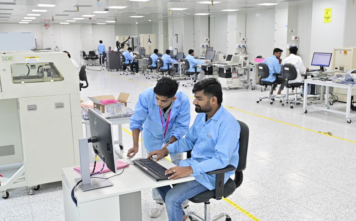
Anuj Grover has compared the process of chip-making to the functioning of a city. Similar to how a city needs architects, masons, carpenters and plumbers to work, chip-making also needs semiconductor architects and designers for the chip to function, he says.
| Photo Credit:
Murli Kumar K
The city parallel is not an exaggeration. Chips are so sophisticated that a microscope can literally only scratch the surface: layers upon layers of circuits criss-cross any given chip, with billions of individual transistors packed into a single unit. There is a reason that few countries have a lead in fabricating chips: this is a technology that requires precision equipment that is so sensitive that even slight impurities in water, or practically undetectable fluctuations in the electricity powering the equipment, can ruin the yield of a production run.
Easier access to software
The Union government, as part of the Indian Semiconductor Mission’s Chips to Startups (C2S) programme, purchased licenses in bulk for software suites of the major EDA tool developers: Siemens based out of Germany, and Cadence and Synopsys in the United States. Dozens of colleges in India have access to those tools now, and a dashboard maintained by the government shows that cumulatively, students have logged millions of hours on those tools.
“We were paying ₹3–4 lakh a year in renewal fees before the C2S program,” Nilima Warke, a professor at the privately-run VES Institute of Technology says. And that was just for tools from one provider. Now, students and faculty have access to four different toolsets for free. This time around, they’re getting access to “professional bundles” used in the industry, not the more limited academic ones they were previously using.
Warke and one of her colleagues designed a 180 nanometer (nm) chip that is being “taped out” at the Semiconductor Lab in Mohali. While 180 nm chips are relatively large — so-called “legacy” nodes, compared to the “frontier” 3–7 nm chips on most advanced phones — Warke points out that before this, much of the training was academic in nature. In a few years, university students will be working on designs at the frontier level too.”
Even without this kind of software hand-holding, though, semiconductor design firms have seen success already. Tessolve, a design firm headquartered in Bengaluru, has been operating since 2004, with offices in nine cities in India, and operations across 10 other countries. The Hero Group acquired a majority stake in the firm in 2016, and Tessolve announced that it raised $130 million this year. “A lot of the cities we operate out of are Tier-2,” Srini Chinamilli, Tessolve’s CEO says, in an interview over Zoom from Singapore. “There are lots of people who are looking for opportunities in places where they have more emotional connect.” In other words, closer to home.
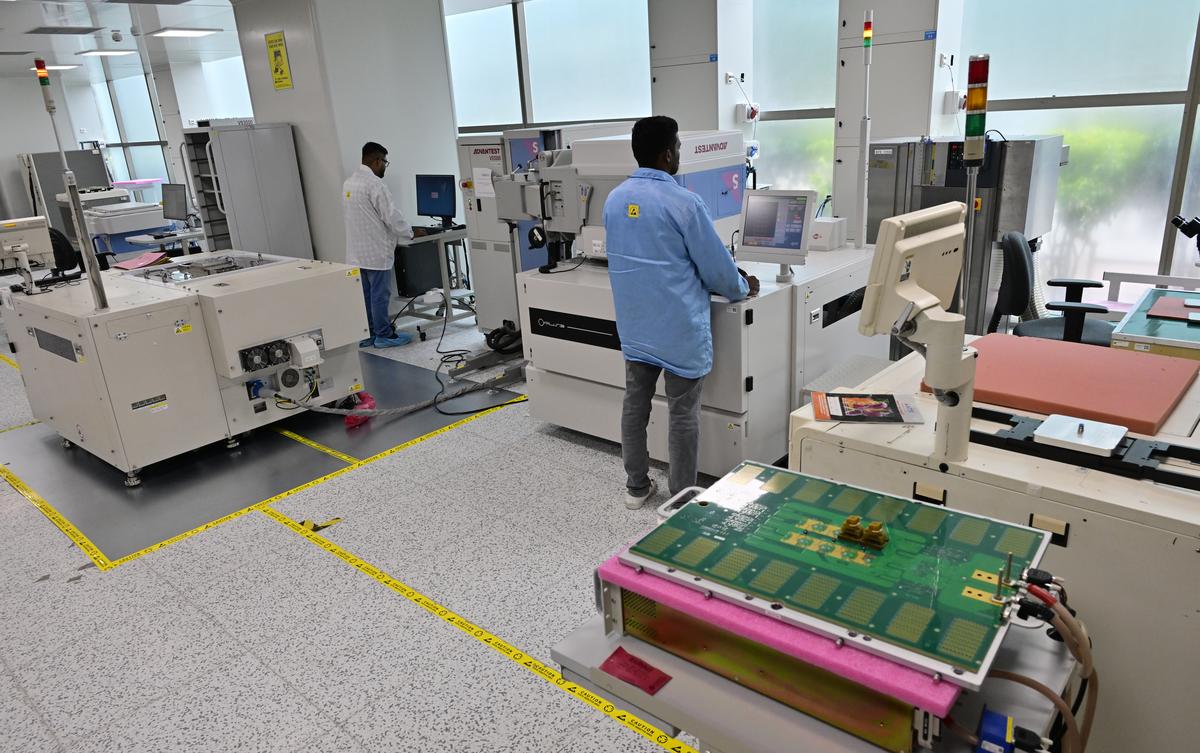
A semiconductor die inspection being conducted in Tessolve Semiconductor in Bengaluru.
| Photo Credit:
MURALI KUMAR K
That has worked out just fine, Chinamilli says, with workers logging in from large centres like Hyderabad and Bengaluru, but also from smaller cities like Visakhapatnam and Coimbatore.
Student-industry gap
“After COVID, the industry got more comfortable working remotely,” he says. So far, so good. Government support has helped somewhat, and the design space is in a good position in India. But Indian chip expertise at the university level is not where it is in the U.S., which has pushed the frontier work. Why is that, and how can we get there?
“Universities should be proactive and tie up with the industry, so that whatever training they are doing is addressing some real problems in the industry, and also addresses what the industry is looking for in terms of employability,” says Chinamilli. Grover couldn’t agree more. But therein lies the rub: “In India, the industry invests only 0.4% of their profits or revenues into academic research and development,” Grover points out. In the U.S. and South Korea, that number is 10-15 times higher. In the U.S., Grover says, academia working with industry wasn’t just making graduates better prepared for industry. The benefits ran far deeper, even for the industry.
Grover invoked the example of another UC San Diego professor, Andrew Kahng, whom he called an “authority” on EDA tools. “And do you know why he was an authority worldwide in EDA tools? Because when I was working in his lab in 2002, Cadence engineers would visit us and say, ‘See, we anticipate that three years down the line, so-and-so problem will arise. Can you start to work on some algorithmic solutions for it?’”
Graduate and Ph.D. students had a ringside view into the chip design’s biggest problems, and would enter the industry with something to contribute immediately, far from needing training. Meanwhile, the EDA tool developers who supported these efforts, such as by paying Ph.D. students’ stipends, would have visibility into preprints, giving them anywhere from a few months to a year’s head start over their competitors, a critical lead to secure in an industry that iterates and improves as rapidly as the chips they produce.
Ph.D. stipends are far cheaper than hiring a full-time employee to work on cutting-edge theoretical problems, but Indian firms largely don’t seem prepared to pay even that kind of cost to advance research and development. “They are perfectly willing to fly down an expert and pay lakhs, even with limited follow-up,” Grover complains.
Another large IT company, he says, asking for it to not be named, balked even at a below-standard rate for sponsoring a Ph.D. candidate working on issues that were directly relevant to the firm. And multinationals have no compelling reason to work with Indian academics beyond narrow areas already handled in the country: “Why would a French company sponsor Indian Ph.D.s,” Grover asks.
There is a larger issue of the electronics ecosystem in India, Grover says, bemoaning the industrial base of even simple components being hollowed out. “There was a time when Indian companies were exporting supercomputers to countries like Germany and the U.S.,” he says. “Now, even the controller inside a ceiling fan is being imported.”
A bigger problem
All said and done, though, the chips themselves are not the most valuable part of the electronics ecosystem, Grover says. “What do you think an iPhone’s bill of materials is,” he asks, holding up his teal handset, referring to the price of all the components and their assembly. “It’s just 31% of the price of the overall device.”
The rest of the value, he says, is in design and intellectual property. The benefits of chip design are ultimately a portion of the chip value, which is itself a part of the bill of materials. To take full advantage of the ultimate value of these components, he says, India has to become a “product nation”, and actually create things that the world wants to buy. And design is a key part of that. “Even the button placement on this phone is patented,” he points out.
The good news is that as far as design and hardware testing are concerned, hiring hasn’t let up. One BITS Pilani graduate noted on social media platform X that over 60 students were picked up in placements by NVIDIA (“BITS Pilani NVIDIA campus,” he quipped). This is even as other parts of the tech industry reel from a slowdown.
“Now, it’s only about the will,” Grover says. “The ingredients are all around us.”