






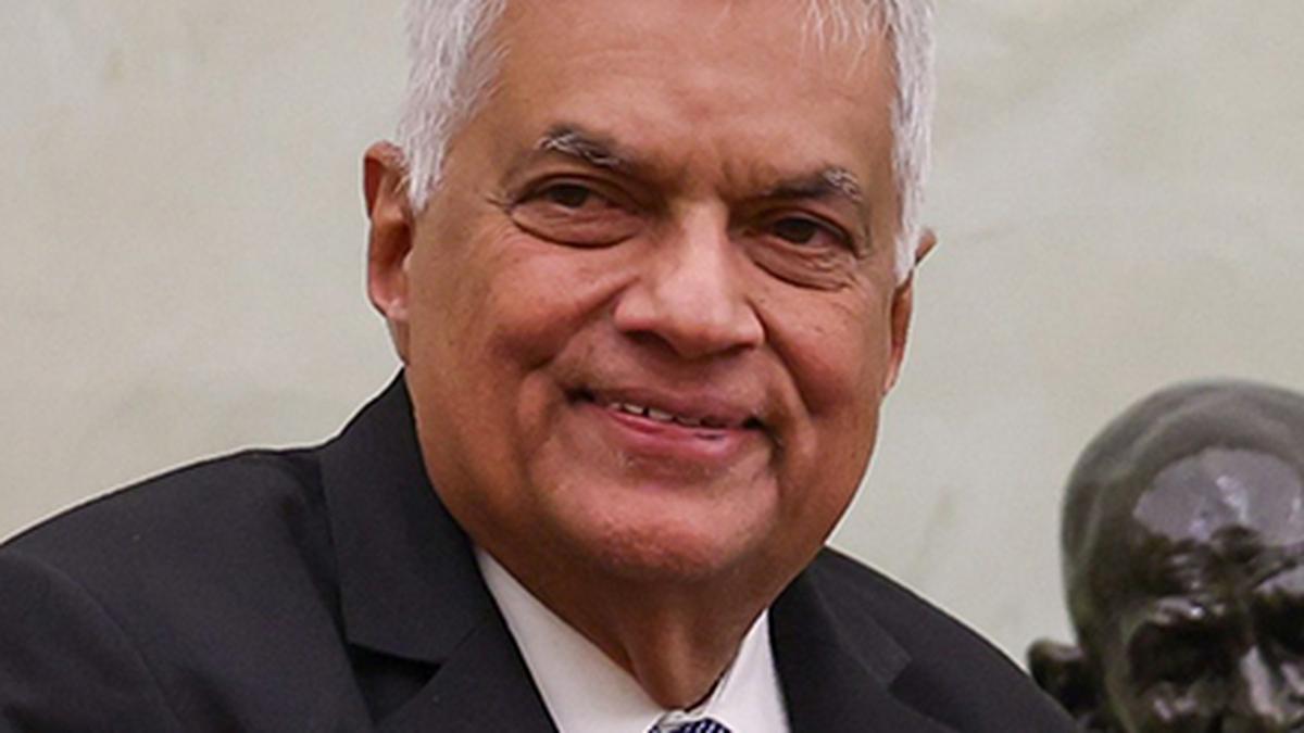

India needs to strengthen capabilities across the semiconductor value chain, from manufacturing and materials to research and specialised skills, to reduce dependence on foreign technologies and build a resilient domestic ecosystem, Dr. Kamaljeet Singh, Director-General of the Semiconductor Laboratory (SCL), Mohali, said on Tuesday (October 27, 2026).
Speaking at the inaugural session of the Semiconductor Summit 2026, organised by SRM Institute of Science and Technology in association with The Hindu, he said India had a significant presence in semiconductor design but remained dependent on foreign suppliers for critical inputs, including electronic design automation (EDA) tools.
“But the EDA tools which we are using also come from the U.S. So that is why all dependencies are foreign,” he said.
Mr. Singh said the country needed to overcome several challenges to become a technological power. “Technology is one of the challenges, talent is one of the challenges, resources is one of the challenges, time is the challenge, acceptability is the challenge and capital is the challenge,” he said.
He said India needed to build capabilities not only in chip design and fabrication but also in the supporting supply chain, including manufacturing equipment, raw materials, chemicals, gases and packaging materials. Semiconductor supply chains were concentrated in a small number of countries, making access to these inputs critical, he said.
India’s semiconductor requirements were substantial, and the country needed to manufacture more of the chips it used domestically, Mr. Singh said.
Research and manufacturing
He highlighted the need to connect research with manufacturing, arguing that developing semiconductor technologies required researchers, pilot lines, manufacturing facilities and industry participation.
“You need a lot of researchers to come into place, you need a manufacturing unit, you need a lot of technology to be developed to attain the system design and architecture,” he said.
Mr. Singh said the India Semiconductor Mission had supported the development of domestic capabilities. Under the first phase, ₹76,000 crore had been pumped in, with 12 projects approved, five of which had been operationalised and another expected to become operational, he said.
The second phase of the mission had six pillars, including chip design, manufacturing, materials and machinery, with research and development and skill development added as two further areas of focus, he said.
He stressed that India needed to strengthen specialised engineering and manufacturing capabilities alongside its existing design talent.
Making chip design accessible
Mr. Singh highlighted SCL’s efforts to make semiconductor design education more accessible through open-source tools. The laboratory had integrated its process design kit (PDK) with open-source tools so that students unable to afford commercial EDA software could learn chip design.
“Any student of tier 2, tier 3 city can sit at his home and can learn chip designing. We are facilitating fabrication also,” he said.
He said SCL was also working with academic institutions and startups and had introduced training programmes, internships and faculty development initiatives.
The laboratory had supplied more than 50,000 chips to strategic and commercial sectors over the preceding two to three years, with no field failures reported to date, he said. SCL also supplied chips for space programmes, including Chandrayaan-3, and was working towards developing integrated solutions combining sensors and chips with software and firmware.
Integration gains importance
Mr. Singh said the semiconductor industry was increasingly focusing on integrating different types of chips as conventional transistor scaling became more difficult. Advanced packaging and chiplet-based designs could help improve computing capabilities by connecting different components.
“Nowadays, I think transistors are saturated, the size is saturated, and a lot of things are coming in the packaging,” he said.
He said future development would also involve technologies such as photonics, quantum computing and power-aware design, requiring closer collaboration among academia, industry and start-ups.
“Because the leader will be the one that learns the fastest from every wafer, every test, every failure and every experimentation,” he said.
Published – October 27, 2026 06:01 pm IST