


Computers denote data in bits – the famous 0s and 1s – using semiconductors. These are small physical devices that store these values and perform mathematical operations on them. The sum of all these operations is what allows the computer to compute.
We have powerful computers almost everywhere around us thanks to a technology called semiconductor lithography – the science of printing intricate circuits with extreme precision.
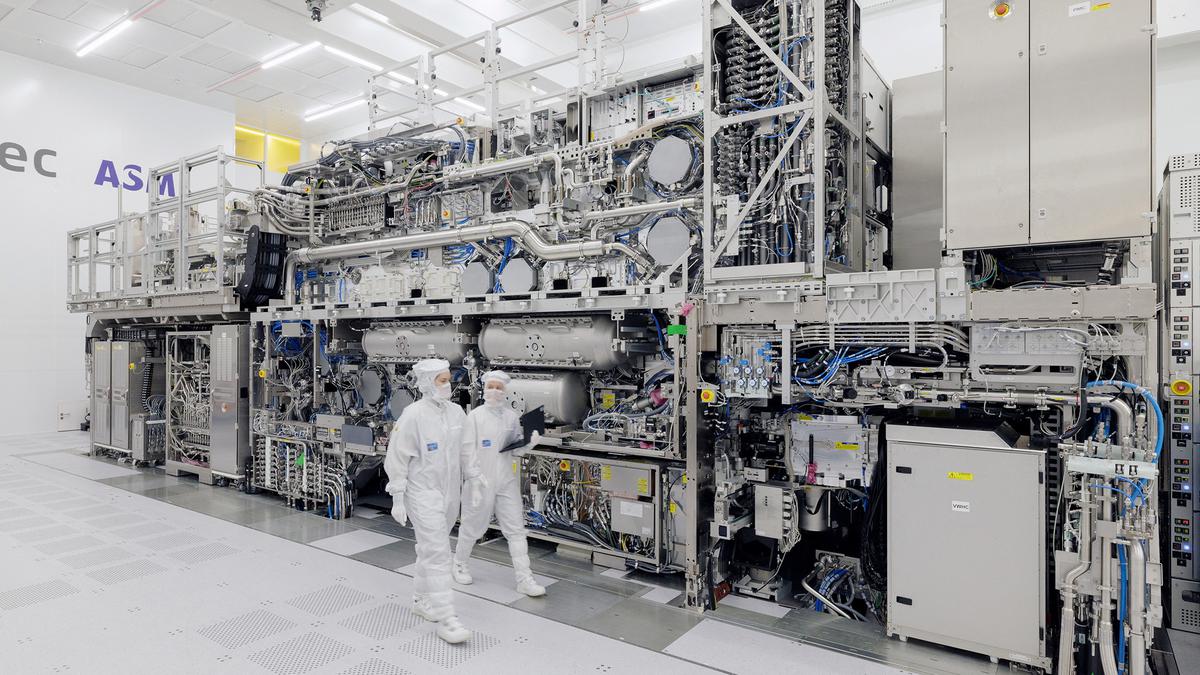
There are machines that automate this process, at a cost of anywhere between Rs 800 crore and Rs 1,600 crore. Only one company, ASML, headquartered in the Netherlands, makes them, giving it an absolute monopoly in a market worth $125 billion and rendering it the technology company with the highest market value in Europe.
In February, ASML unveiled its new ‘High NA EUV’ machine. It costs $350 million (Rs 2,900 crore) apiece and is as big as a double decker bus. Industry analysts say the machine ups ASML’s competition with Intel in the market for the most advanced semiconductors, to power the next generation of computers and smartphones.
This machine uses extreme ultraviolet (EUV) photolithography, a next-generation technology, to make the semiconductors. Here, simply speaking, the mould of the circuits of a transistor – a type of semiconductor – are transferred to a silicon wafer coated with a light-sensitive material called a photoresist. When light is shined on the photoresist, the mould solidifies and its gaps can be filled with wires to form the transistor.
What is the Rayleigh scattering criterion?
The smallest feature size that can be moulded on the silicon wafer is governed by a physics principle called the Rayleigh scattering criterion. According to this criterion, the size of the feature to be projected on the wafer is proportional to the wavelength of light used and inversely proportional to the aperture of the lens that collects light before projecting it onto the wafer.
The proportionality with the wavelength of light includes a factor called ‘k’. Its value depends on many factors, including the operating temperature and the chemical properties of the photoresist, but has a maximum value of 0.25. In the inverse proportionality, the aperture indicates the amount of light that can be collected and focused on the wafer: the greater the aperture, the smaller the feature size.
In most cases, engineers have reduced the smallest size imprinted on the wafer by reducing the wavelength of the light shined on the photoresist. Around four decades ago, for example, chip-manufacturing companies used light of wavelength 436 nanometres (nm); the latest machines of today use 13.5 nm light, which lies in the extreme-ultraviolet (EUV) part of the electromagnetic spectrum.
Just before EUV machines, chip-makers relied on deep UV light (193 nm wavelength) to project intricate patterns onto the wafers.
How is EUV light produced?
When this process is repeated multiple times across the whole wafer, the end product is an integrated circuit, a.k.a. a chip. The dominant way to make more powerful chips throughout history has been to increase the number of transistors crammed on the chip. This in turn requires the size of the transistors to become smaller, motivating innovation in reducing the wavelength of the light used to make the moulds. But this is much easier said than done.
Consider the process that the ASML machine (likely) uses to produce 13.5-nm light. First, a gun shoots a spherical droplet of liquid tin, around 50 micrometres wide (half the width of a strand of hair), at nearly 300 km/hr into the machine. In flight, a laser strikes the tin and deforms its shape into a pancake. This tin pancake is still in flight when another intense laser beam strikes it, transforming it into a hot, ionised gas with a temperature 40-times higher than that on the surface of the Sun. At this juncture, the gas emits EUV light that the machine collects for use.
This entire process – from the gun to the emission – happens 50,000-times per second to produce EUV light of sufficient intensity. That is, the guns shoot 50,000 tin droplets per second and there are twice as many laser shots to modify it. This process also unfolds within a vacuum because virtually anything, even air, absorbs EUV radiation, leaving less for the machine.
How precise is the machine?
The mirrors used to collect and reflect the generated light are a marvel as well. Crafted by the German company Zeiss, they boast the smoothest surfaces ever created by humans. Approximately 30 cm wide, their surfaces are so flawless that if scaled to the size of Uttar Pradesh, the tallest bump on each surface would be a mere 1 mm high. This is a level of imperfection lower than the size of a single atom.
Similarly, the mirrors reflect EUV light with such precision that if aimed from the earth, they could strike a cricket ball on the moon and not miss by more than the width of a strand of hair.
Finally, this light has to be guided to the silicon wafer with similar precision, which requires the wafer to be moved in increments as big as the smallest features to be printed on it. To achieve this, the stage holding the wafer floats on a magnetic field, to avoid any friction-induced compromise in precision. Ultra-sensitive sensors then adjust the wafer’s position 20,000 times per second, with an accuracy nearing just 50 picometers. This is like adjusting the earth’s position in space by a distance of one fingernail at a time.
All these 20,000 adjustments are executed with an acceleration greater than that of any F1 car or a fighter jet, to increase the device’s production efficiency.
What is the machine’s value?
As such, ‘High NA EUV’ doesn’t represent a single achievement but a collection of multiple achievements, brought together to push the boundaries of computing just enough to create the next generation.
Our future is being constantly reshaped by artificial intelligence, robots, intelligent automobiles, high-quality digital communication, powerful gadgets, and space exploration. These innovations are not only transforming the way we live and work but also opening new possibilities that were once in the realm of science fiction. The fundamental enablers of these revolutions are semiconductor chips, which carry out the enormous numbers of calculations required to materialise these technologies.
By continuously making these chips smaller, faster, and more efficient, we have gone from just four transistors in the first integrated circuit in 1948 to more than 19 billion in the chip we use in our smartphones. This innovation is driven by Moore’s law, which describes the expectation that the number of transistors on a microchip will double approximately every two years.
Lithography machines also have strategic ramifications. For example, ASML is not allowed to sell its lithography machines to China along with other components, to prevent researchers in the Asian country from potentially reverse-engineering them. So these machines underscore the fact that major technological breakthroughs can provide highly skilled jobs as well as strengthen a country’s standing in the geopolitical arena.
Awanish Pandey is an assistant professor at IIT Delhi with the Optics and Photonics Centre.